This is part 4 of the following series:

  1. Originating requirements
  2. Use cases
  3. Product requirements specification
  4. Physical architecture and interfaces (this document)

The document maps all specifications to hardware or software interfaces. To contribute more contents, identify all external interfaces and describe all properties that meets the system-level specifications: mechanical / optical / electrical / softrware. Omit all internal interfaces; those should reside in code comments or in the technical reports.

How to use this document

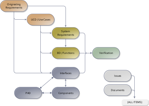
This document follows the Product Requirement Specifications (PRS), where the interfaces linking various sub-systems are captured.

There are also lower level internal interfaces; these are often the interfaces that are owned by a single engineer (e.g. the electrical interfaces found on a single circuit board). These lower level interfaces are not given a number and description, are not turned into requirements, and instead are captured in lower level specifications and design documentation.

System engineering V-model. Component-level designs are captured following the system-level specifications.

Similar to defining use cases, the process of capturing the architecture via a Physical Architectual Diagram is helpful to ensure that the interfaces are identified. For particularly complicated interfaces, the descriptions above can reference a more detailed document (such as a mechanical interface drawing, electrical pinout, firmware/software communication protocol, etc.).

The Logical Architecture Diagram (LAD) groups the functions into sub-systems. Flows among functions are mapped to Interfaces, featuring interactions among sub-systems. The LAD is in turn implemented by physical components in the Physical Architecture Diagram (PAD). The PAD links all external interfaces with the corresponding internal components of the system.

Interface specifications are traced back to the Originating Requirements, and are verified by the Verification Plans. The Physical Architecture Diagram (PAD) links all external interfaces with the corresponding internal components of the system.

Logical architecture

This section is intentionally left blank.

Physical architecture

pad-1: Power

A power port accessible by the user and used to charge the device.
Charging subsystemData port[int-2] Front panelint-3Power port[int-1] Power interfaceLEDsDevice housingPCBComputerUserPower supplyuseuseuse
Component diagram "pad-1: Power"

int-1: Power interface

The device connects to a power supply via a connector for charging.

Satisfies:

  • [sys-1] Charge duration:A battery with <5% capacity shall charge to >95% capacity in <5 hours.

Mechanical description

  • The power interface shall be a micro-USB power connector.
  • The power supply shall contain the plug, the device shall contain the jack.

Electrical descriptions

  • The device shall receive 1A max, 5V +/- 25mV via the power interface.

int-2: Front panel

The device has a physical port on the front panel for charging.

Satisfies:

  • [sys-2] Charge indicator location:The charge indicator shall be located 1.0 +/- 0.2 cm from the charging port.

Mechanical description

  • LED shall fit a 3.1 mm diameter hole on the housing.
  • LED shall be yellow in color.

Electrical descriptions

  • The LED shall receive forward current 20mA.

Software / firmware descriptions

  • The LED shall be blinking at 2 second interval.