Optics
Optical system design, as a business, has become very costly to run over the past few years for freelancer CDM (contracted development & manufacturing), especially without purchasing authority and a host lab to support the R&D. Nowadays, I mostly compose/evaluate optical schematics, and verify them against OEM-provided specifications. If you find anyone who wishes to ship the instrument on loan to my office, I am more than willing to pick up the slack. Please feel free to contact me on LinkedIn.
Optical design review services:
On-axis confocal free-space / few-mode fiber optics design, optimization, and fabrication;
Common path multi-modal imaging path design and characterizations; (quantitative) phase contrast, widefield fluorescence, confocal, and structured illumination;
High-power (up to 3,500 milli-Watt) illumination optics prototyping (i.e. Research-grade only, not for commercialization);
System integration with real-time compute engines (mostly Nvidia Ampere micro-architecture) and beam-steering electronics (electro-optics or acousto-optics of up to 400MHz bandwidth).
Conduct trade studies and architecture tradeoff analysis among various imaging modality; foundational optical modelling with either Fraunhofer/Poisson/Fresnel approximations.
Professional optics design & fabrication
Plastic molded microscope lens for 96-well parallel microscope
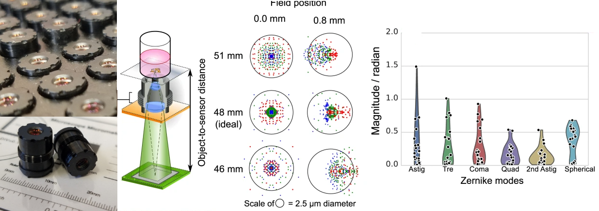
Originally conceived by Dr Changhuei Yang and his PhD student, we spec’ed out the optical magnification, field of view, and focal shift requirements from the 96-CMOS camera project. When I took over the project, I reviewed the manufacturer provided CodeV raytracing report, provided expert’s feedback, and then validated the lens and the specifications with the Caltech-patented aberration extraction algorithm to analyze the Zernike coefficients.
A.C.S. Chan, J Kim, A Pan, H Xu, D Nojima, C Hale, S Wang, C Yang, “Parallel Fourier ptychographic microscopy for high-throughput screening with 96 cameras (96 Eyes)” Scientific Reports 9, 11114 (2019).
Patent: US 20190137753
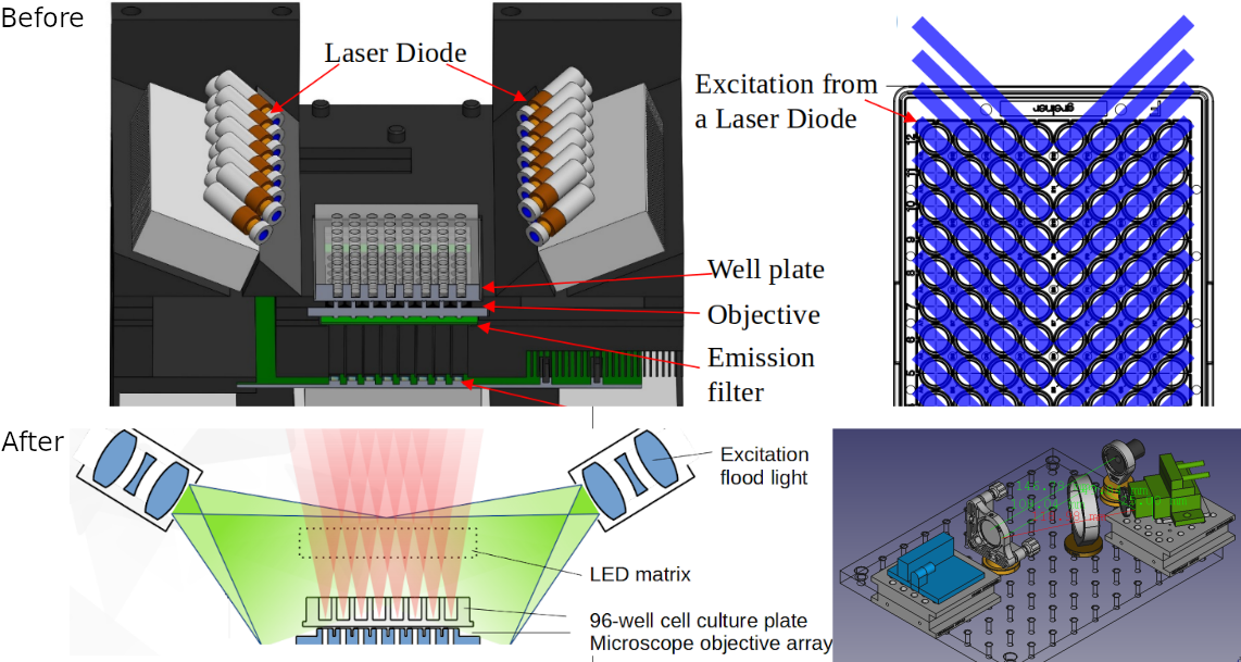
2-Laser illumination engine for whole-plate fluorescence excitation, 7000 milliWatt per plate
Laser pointers are often a foolproof solution for early instrument prototyping, as obtaining laser safety clearance is relatively easy. R&D can be accelerated due to their short lead time, as well as by bypassing the need for laser driver circuit procurement.
However, it often makes sense to re-architect the illumination optics to improve thermal stability, illumination homogeneity, and ease of optical alignment. I assisted the original project owner in completing the evaluation phase of the early prototype. Upon the scheduled disassembly, I reached out to stakeholders to re-capture the design constraints, followed by designing a new system architecture for hardware, firmware, and optics to meet the updated requirements. The laser pointer-based design was replaced with an external light engine, coupled with homogenizing light pipes and off-the-shelf (COTS) projection optics. I also custom-designed the thermal solutions, laser driving electronics, and laser monitoring firmware, which interfaced with the main instrument control board via the I2C bus.
The context
For a 6-well multi-modal imager (i.e., quantitative phase and widefield fluorescence), it makes sense to design the illumination optics with one laser diode per well per channel. This allows individually addressable laser driving electronics to minimize photodamage to live cells. Having independent laser power controls also provides greater flexibility in laser power calibration, simplifying downstream cross-well data normalization pipelines.
As researchers transitioned from the 6-well plate to a 96-well configuration, the logical approach was to replicate success by simply “copying” the design over. In fact, first-generation overhead projectors and concert lighshows replaced halogen lamps with laser diode knife-edge arrays to maximize the power-to-weight ratio. However, when we packed 30 laser pointers into the prototype, we quickly encountered multiple issues that caused significant system downtime, including thermal overload, laser driving current variations, mechanical misalignment, and uneven illumination.
It is worth noting that the original prototype—simply mounting 30 individual laser pointers—was a victory from the primary stakeholder’s perspective. Paraphrasing a fellow R&D scientist’s words from Turning Science into Things People Need: Voices of Scientists in Industry:
A constantly failing instrument performs exactly as designed—it stays online just long enough to capture R&D data for analysis before falling apart the next (milli)second. This proves that we don’t pay for what we don’t need in scientific discoveries.
Nice to have features If I had sufficient funding, I would have contracted the design to specialists in off-axis darkfield trans-illumination optics. I also would have been bolder in exploring freeform reflective optics—after all, what we truly need is a pair of rectangular floodlights illuminated at a shallow angle.
The 96-camera system concept was also ahead of its time by at least a decade. The DPSS laser diode array (465 nm, ~35% fluorescence quantum efficiency) would have been superseded by a stacked GaN diode array at the wafer level (488 nm, 80% fluorescence quantum efficiency), completely bypassing the optical pumping setup and the bulky diode package.
A.C.S. Chan, J Kim, A Pan, H Xu, D Nojima, C Hale, S Wang, C Yang, “Parallel Fourier ptychographic microscopy for high-throughput screening with 96 cameras (96 Eyes)” Scientific Reports 9, 11114 (2019).
4-channel Peltier PID cooler for 3.5Watt laser modules, 30W per channel
All-optical spatial light modulator for structured illumination at 10 million FPS
The holy grail of a spatial light modulator (SLM) is to bypass all mechanical actuators in pursue of speed. At >10 million FPS range, the MEMS technology can no longer meet the requirements. I designed, modelled, and validated the all-optical SLM design on a physical optical setup.
Due to the cost prohibitive manufacturing and cleaning process of the thin-glass optical cavity (VIPA), I coded an optical simulator based on wave propagation optics, and optimized the SLM design parameter (e.g. thickness, reflectance, core material) based on multi-objective genetic algorithm (MOGA). The optimized design is successfully fabricated, assembled, and validated on a physical system.
Acousto-optic beam deflection at 1 million sweeps per second for pixel super-resolution
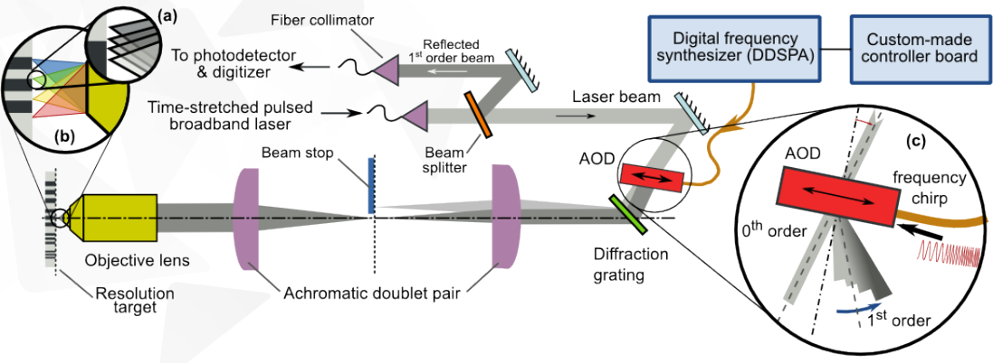
Under the lead of Dr Terence Wong, I procured the acousto-optic deflector (AOD) evaluation kit and integrated it into his ultrafast imaging flow cytometry system for cancer detection. I brought up the RF wave generator & amplifier module, and designed controller PCBs to synchronize incoming fempto-second laser pulses. I also conducted AOD sweep angle and step size trade studies to further understand the limit of the system.
Amateur optics
Poorman’s pinhole camera with silver-halide films
TBD.
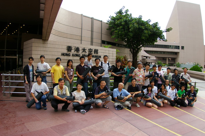
2017 - 2010: Amateur telescope making
Phase 1: Coarse grinding
Phase 2: Fine grinding
Phase 3: Wet polishing with lap pitch
Phase 4: testing for optical aberration
Phase 5: Opto-mechanical assembly
Phase 6: field testing